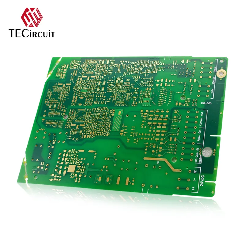
Creating for Effectiveness: Next-Gen RIGID PCB Layout Strategies


In the technology industry, precision and optimization work together with development. When it pertains to printed circuit card (PCBs), the backbone of modern-day electronic devices, efficiency isn't simply an objective-- it's a competitive side. RIGID PCBs, where elements are electrically interconnected on stiff substrates, are at the center of this effectiveness drive, demanding next-gen format strategies to meet the expanding needs of high-speed applications. Right here, we explore some sophisticated layout factors to consider and ideal techniques in stiff PCB design.
Enhancing PCB Layout for Warmth Management
Heat dissipation is a vital factor to consider in the longevity and stability of electronic gadgets. pcb printer with inadequate heat management can cause parts overheating, minimizing their operational life and the overall safety and security of the gadget. A correct design that consists of the tactical positioning of thermally conductive traces, thermal vias, and heat sinks can considerably boost the board's capacity to take care of thermal tons.
Integrating big copper puts and power planes, along with a cautious spacing of elements to allow air flow, are efficient design approaches. Additionally, making use of element thermal pads and thinking about the orientation of the board within the device or room can assist in all-natural convection cooling. An enhanced design also introduces the principle of thermal resistance in very early stages, ensuring that the warm created by vital elements is effectively transported away from the vital locations.
https://tecircuit.com.cn/products/ of Layer Stack-Up Arrangement in RIGID PCBs
The stack-up configuration affects the electric performance and signal integrity of a PCB. It specifies the positioning of power and ground planes, signal layers, and dielectric products, which play a significant duty in regulating resistance, crosstalk, and RF disturbance.
A well-structured stack-up often consists of high-speed signal layers sandwiched in between power and ground airplanes to give constant referral airplanes for signal return courses. Differential set directing and managed insusceptibility tracks can be achieved better when the right layer stack-up is utilized. For inflexible boards, decreasing the distance in between layers can cause lowered layer-to-layer shift effects, which are essential for keeping signal integrity in high-frequency applications.
Signal Honesty Difficulties in High-Speed PCB Designs
In the world of high-speed PCBs, ensuring signal integrity (SI) is extremely important. Poor SI can cause information corruption, efficiency destruction, and the requirement for pricey redesigns. Impedance matching, trace length tuning, and reducing skew prevail methods for SI, but they call for precise interest to detail.
Devices like area solvers and simulation software program can assist in analyzing SI characteristics during the design phase. They assist in anticipating and dealing with issues such as reflections and timing inequalities that can happen at user interfaces and adapters. With high information rates becoming much more common, the demand for rigorous SI evaluation and design recognition techniques has never been more important.
Making Use Of Embedded Elements in RIGID PCBs for Room Conserving
To address the miniaturization fad in consumer electronics, stiff PCBs currently usually include ingrained components modern technology (ECT). ECT includes embedding passive elements-- like resistors, capacitors, and inductors-- directly into the PCB substrate, which not just lowers the board's impact however also reduces parasitics and boosts signal performance.
Embedding components also enhances the board's mechanical effectiveness and dependability by safeguarding the parts from environmental variables. However, it requires a cautious analysis of the mechanical and thermal homes of the embedded materials to make sure that they do not impact the board's honesty or the performance of various other components.
Best Practices for Multi-Layer RIGID PCB Design
Multi-layer Inflexible PCBs are the go-to service for facility and high-density styles. Managing power distribution, managing insusceptibility, and preserving a good ground structure are crucial areas for worry in multi-layer styles. Partitioning the PCB right into power, ground, and signal regions, and utilizing proper decoupling methods, can aid distribute power efficiently and reduce noise on the power rails.
Making certain proportion in the layer stack-up is crucial for keeping controlled impedance, particularly for differential pairs. In addition, taking care of crosstalk by keeping the right spacing and using guard traces can significantly enhance signal top quality. It's also critical to use layout regulations that enable for simple production and testing, such as preserving appropriate clearances and remaining within the manufacturer's specifications for minimal feature dimensions.
In final thought, RIGID PCB design is a multifaceted process that involves navigating different layout restrictions, part positioning, and layer stack-ups to achieve optimum electrical efficiency, mechanical reliability, and thermal monitoring. By applying the most up to date layout techniques and taking into consideration the full lifecycle of the item, engineers can create PCBs that not just work accurately but also add to the total performance and toughness of the last device.