Practical Style Strategies for Gold Finger PCBs


Practical Style Techniques for Gold Finger PCBs
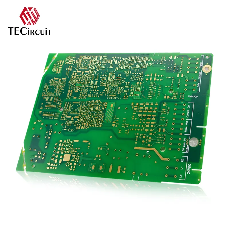
Gold Finger PCBs have actually become progressively prominent across various sectors as a result of their capability to stand up to rust and boost efficiency in extreme atmospheres. They are likewise ideal for applications that call for high-quality electric connectivity such as sd card, graphic cards, and routers. To design a high-quality Gold Finger PCB, you need to understand the fundamentals of the style process to make sure ideal efficiency. In this article, we will discuss vital style strategies that you should integrate to develop a high-quality Gold Finger PCB.
Determining flexible pcb And Size of Gold Finger PCBs
Before you start developing a Gold Finger PCB, you need to figure out the shapes and size of the PCB. The most typical form for Gold Finger PCBs is rectangle-shaped, however you can also pick an extra complex form with contours or rounded corners. As a guideline of thumb, the size of the PCB ought to be huge enough to suit the parts and traces while being small sufficient to fit the application.
Choosing the Right Density for Gold Plating
The density of the gold plating is one more important factor in developing a premium Gold Finger PCB. The density of the gold plating will impact the total performance and durability of the PCB. A thicker gold plating will certainly supply better electrical conductivity and improved resilience but might increase the overall price of the PCB. On https://tecircuit.com.cn/collections/ , thinner gold plating may lower the total expense of the PCB however may endanger on performance and toughness.
Layout Considerations for Gold-Plated Get In Touch With Fingers
When developing Gold Finger PCBs, you have to take into consideration the layout of the gold-plated get in touch with fingers. The contact fingers must be developed to supply optimal electric connectivity and sturdiness. One design factor to consider is to make sure that the fingers are long enough to handle duplicated insertions and eliminations from the adapter. Additionally, you have to guarantee that the fingers are broad adequate to offer sufficient conductivity and withstand wear and tear.
Picking the Appropriate Substrate for Gold Finger PCBs
The substratum of the Gold Finger PCB is an essential factor in the general performance of the PCB. Usual substratums used in Gold Finger PCBs include FR4, Polyimide, and Rogers. When picking a substrate, you need to think about the application needs and the electric residential properties of the substratum. For circumstances, if the PCB will be subjected to severe temperature levels or chemicals, you must select a substratum that can endure such conditions.
Kinds Of Gold Plating for Ideal Electrical Conductivity
There are numerous kinds of gold plating readily available for Gold Finger PCBs. One of the most usual kinds are Electroless Nickel Immersion Gold (ENIG) and Electrolytic Hard Gold (E.H.G). ENIG is a two-layer plating procedure that entails depositing nickel onto the PCB before adding a layer of gold. ENIG uses superb solderability and conductivity and is ideal for high-density PCBs. E.H.G involves transferring a thick layer of gold onto the fingers, making it perfect for applications that call for high-wear resistance.
Designing a high-grade Gold Finger PCB requires mindful factor to consider of a number of vital elements such as size, form, substrate, thickness of gold plating, and layout factors to consider for the gold-plated contact fingers. By complying with these layout strategies, you can ensure that your Gold Finger PCB executes optimally and offers enhanced durability. As constantly, it is necessary to follow sector standards and best methods when designing any kind of kind of PCB.